During the ’60s and ’70s, the early mainframe computers and Telcom switches used complex dense wire-wrap technology. High-circuit-count copper backplanes and midplanes often relied on wire-wrap point-to-point, or pin-to-pin layouts. This involved lots of hook-up wire and singular micro-coax for the clock circuits.
The wire-wrap pin backplane connectors at that time typically had round-wired edge contact on the reverse end. In fact, I recall designing some of these using hand tools at DEC Maynard, MA, though the company eventually semi-automated the process with an X-Y automated wire-wrapping machine.
A few years later, computer backplanes were fabricated as printed circuit boards (PCBs), manufactured with layers of woven fiberglass and copper trace circuits. Today’s high-end server or switch PCB backplanes require 30 to 40 manufacturing fabrication steps and 28 to 50 (or more) layers of HDI circuit construction.
By the 1980s and into the ’90s, the optical transport routers/switches backplane and midplane designs evolved to incorporate between 1250 and 2500 individual optical-fiber circuits, with 40 to 80 high-circuit-count optical connectors. These were usually MPO types.
There were also customized 28 fiber-sheet sub-assemblies. These were fabricated into one complex, customized connector optical backplane or midplane harness.
Different fiber sheets are manufactured separately using, for example, pre-formed and pre-ribboned colored buffered fibers with large, circuit-count fiber elements. The fibers are taped at the centered ends, matching the connector location and point-to-point, customized schematic. They are, then, terminated at each end with the correct ferrules and connectors.
The above chassis example could use 14 to 28 fiber-sheet subassemblies, which are connectorized and harnessed together. This type of manufacturing requires expert technicians and jigging equipment that can support asynchronous circuit layouts. So, there are additional labor costs with this technology.
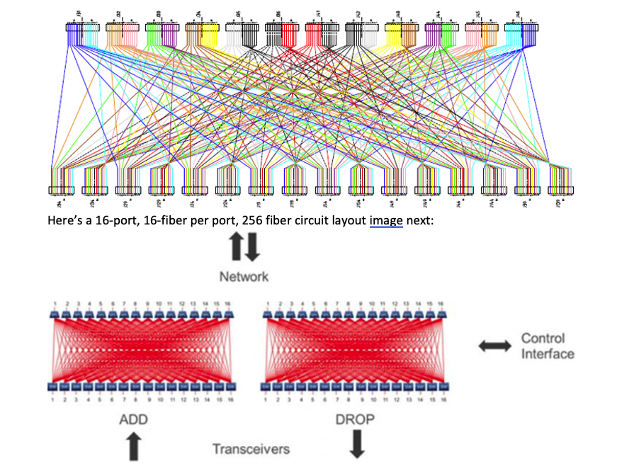
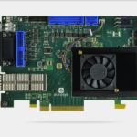
Currently, a 4000+ fiber-circuit designs are in the research and development phase. TE and Rosenberger have such products and processing capabilities, as shown below.
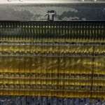
Newer, NxM crossbar and cross-point optical switches use high-port counts and fiber circuits — and, usually, hundreds. Some have benefitted from the X-Y-Z multi-fiber, feed-out mechanism using a single processing tub or pan. That is sometimes referred to as the “X-Y shuffle machine.”
These machines have increased capabilities. Typically, colored buffered fibers are automatically laid out onto an adhesive Kapton or silicone mold. The fiber-ends are held in tight alignment with dimensional control, using temporary processing clear tabs, until the optical ferrules and connectors are terminated.
A typical assembly drops into a switch box with the optical connectors mounted on the internal faceplate areas.
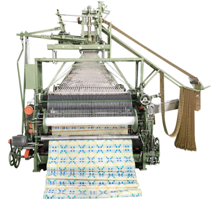
A Jacquard rapier loom could also provide a volume production-process method for this type of inside-the-box, optical-mesh interconnect. It’s possible to automate all of the connectors for mass-fusion terminations, with 8, 12, or 16+ fibers at a time, using a rotating fusion head or multi-headed fusion machines.
Between the 1990s and 2010, DARPA and DoD fly-by-fiber or fly-by-light technology and production contracts primarily supported the development and deployment of advanced high-fiber circuit count, optical communication, and computing switches and systems. Shipboard optical networking equipment was also produced with extremely long and woven fiber designs.
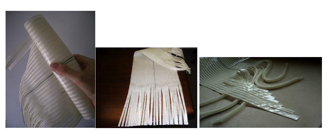
The substrates of the woven fabric sections have varied, including very rigid, rigid, semi-rigid, semi-flexible, and very flexible options. They’ve been used for strong and lightweight cables, routed and layered fiber-circuit boards, or FCBs.
Glass data fibers or fiberglass structural element filaments with silicon-based substrates proved ideal for optimizing the thermal-cycling performance, with a similar coefficient of expansion numbers.
Woven fiber-optic cables with different silicone-based substrates were also designed, qualified, and produced in the ’90s and 2000s. The same with harnesses, motherboards, backplanes, midplanes, sideplanes, baseplanes, and topplanes.
This generation of Telcom and industrial automation systems also used woven-fiber circuit-board assemblies, as well as standard and customized optical midplane connectors for the high-end machines.
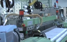
To achieve higher volume manufacturing and lower costs, most automated design options for the woven-fiber circuit interconnects were produced on looms and in-line molded or extruded substrate process linear tubs. In-line, long product testing hoods were also used.
Embedded mil-aero and industrial automation computer backplanes were also fabricated with similar woven glass-fiber looms and substrate equipment. Typically, it would take two or three people to operate a full production build, with little setup and process time. This is especially true in comparison to the older, high-fiber count designs and technologies.
To save on weight, size, and costs, cladded fiber was often used. Other times, buffered and jacketed fiber was preferred.
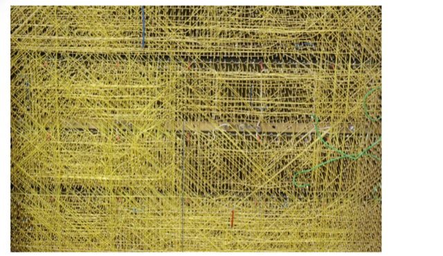
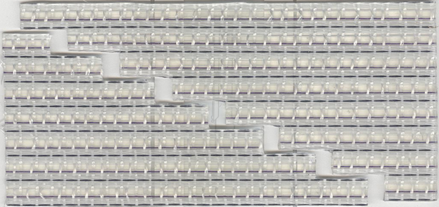
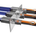
The image below is of an embedded, dual-star optical backplane with woven elements after fiber prepping and black rectangular connectorization.
This symmetrical point-to-point design used switch hubs on both ends. Precision lasers were employed to trim skim coats, regular jackets, or thicker substrates. The lasers were used for glass-fiber prepping and trimming, as well as for fiberglass filaments. Bendable fiber types were preferred for low-loss angled routing.
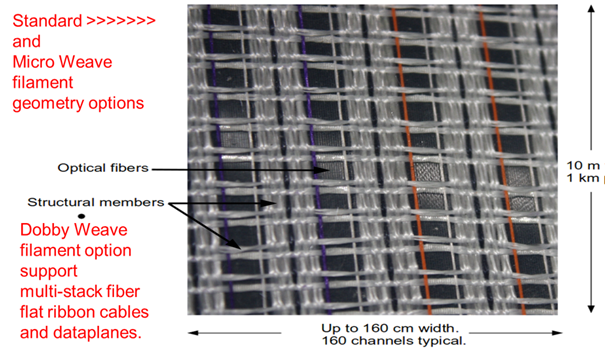
The choice of 8, 12, 16, or 32+ data-fiber, per-link connectors could be programmed with this automated electronic loom machine. The fiber could also be on different center-to-center geometries relative to the active optical chips and connector ferrule interfaces. The machine also supports the use of different fiber diameters.
For instance, an inverse pyramid configuration could support center-hub backplanes and storage module drop-down systems.
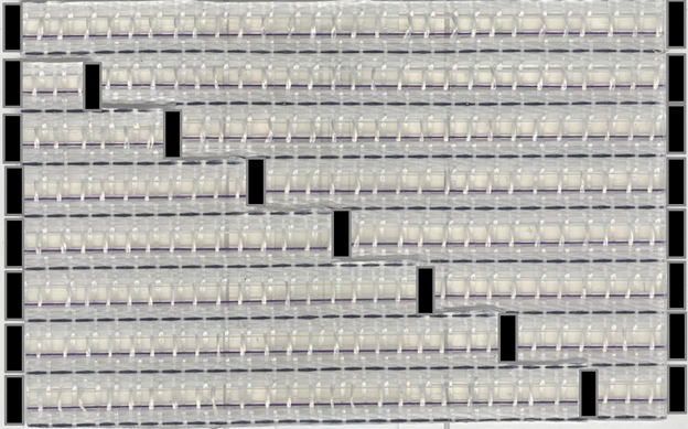
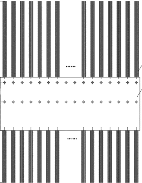
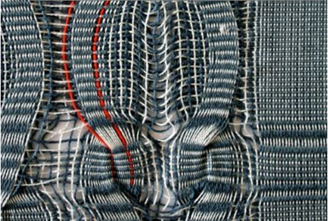
Now check out the images below of the same dual-star backplane with woven elements before fiber prepping and connector termination. There are eight connectors terminated on each end, with eight additional multi-fibered ferrules. There are also six connectors terminated on each internal stepped-end, with 16 or 32 fiber double-stacked ferrules.
In this case, MPO, MTP, and MXC connectors are typically used. These images are examples of very rugged fiberglass filaments and silicone substrates. Other designs could be much larger, providing higher density solutions.
Today’s options
Fiber-type options include the G.657.A2 high-security, solid-fiber hollow-, multi-, and round- or rectangular-core, as well as the POF. Newer, smaller fiber sizes and BIMM types of fiber are now available to support today’s higher density and asymmetrical fiber-circuit layouts. Small, gage-power or control hookup wire, micro-Coax, and micro-Twinax elements can also be woven into fabric.
Additionally, micro-tubing is available for liquid coolant, which is used for modules or chips with standard or medical-grade liquid bearing connectors. Skim coats and thicker substrates might also rely on low-friction coating to aid in assembly and installation. Full mesh, quad star, orthogonal, and other optical data-plane architectures can now be produced with single or multiple-level, skim-coated fiber sheets that are molded together.
Jacquard programmable automated looms can be used to manufacture radiused and angled woven wafts and wefts that support data fibers and other elements.
The FCB and FCBA next-generation developments can be supported by using a combination of Rapier and Jacquard glass-fiber programmable weaving looms. Fiber-circuit layouts are often more streamlined. The designs are application-specific and either more standard and symmetrical or dense and asymmetrical application-specific — while employing thousands of circuit fibers.
New designs typically involve connecting many active silicon-photonic chiplet modules and ASIC optical chips. Advanced designs will likely use SN, SN-MT, and AirMT optical connectors, which are commonly used with newer, pluggable transceiver modules. The miniature looms can create smaller-sized, optical circuit layouts with tiny fibers (similar to tatting laces) for handheld devices.
Summary
Woven fiber circuit-board technologies require close attention as the technologies advance to include higher circuit-count optical computing and network solutions. The supply chain is also worth considering. The quartz sand used for data fibers covers about 27% of the earth’s land surface. It can be resourced from several different countries and is easy enough to prospect. However, the copper used is more difficult and costly to mine.
Overall, woven fiber-circuit boards can enable advanced, inside-the-box connectivity applications. Though it might be better to use a circular or round optical transmission structure within the whole link system to maintain performance and an affordable budget. At least, this seems preferable to the potential challenges with multiple, round-to-rectangular (or flat) optical circuit transition zones and asynchronous geometry — which could easily lead to link losses or latency delays.
It also seems that large circuit boards and internal optical chip-to-chip, chip-to-modules, chip-to-IO faceplates or midplanes will be key to the success of 212, 224, and 256G per-lane speed rates and increasingly higher-speed applications.
Expect design automation CAE and CAD tools that use DFT and DFM principles to develop further to create woven fiber fabric, high-circuit-count FCBs and FCBAs.


Leave a Reply
You must be logged in to post a comment.