Datacenter server processor chips have proven valuable as pluggable and removable devices for the socket connectors mounted to a server’s main PCB board. However, the number of contacts per socket connector has dramatically risen over the last few years. New chips offer 3000 to 5000 or more contact pads per flip chip.
Typically, the socket connector is a BGA SMT mounted directly to the server board and combined with a frame support structure.
Some of the more recent processor chips, chipsets, and chiplets are directly attached to unique substrates, forming a high-performance module board assembly that can be connected to the main PCB board. This is done with a high pin-count socket connector, such as an SMT solder ball.
Application changes
Intel’s newest generation server, the Xeon Sapphire Rapids 7nm CPU chip, still uses an FC LGA 4677 (Flip Chip Land Grid Array) socket connector. The company has successfully used LGA sockets for several CPU generations, so it’s sticking to what works.
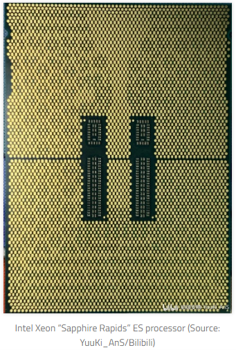
The new chip has 4677 contact pads that plug into the LGA 4677 socket connector using compression-beam copper contact tabs. The image below showcases the CPU’s complex contact pad array. It maintains excellent signal integrity when going through thermal cycling and vibration.
Intel’s previous generation of Xeon flip chips used contact pads, which plugged into sockets such as the LGA 4146 and LGA 4189, using 2092 and 4200 contacts positions. We’ll have to see if Intel’s future Emerald Rapids chips also use the LGA 4677 sockets. Newer 3nm Intel Xeon chips, and other large chips, will likely require around 3300 to 5300 LGA contacts per socket.
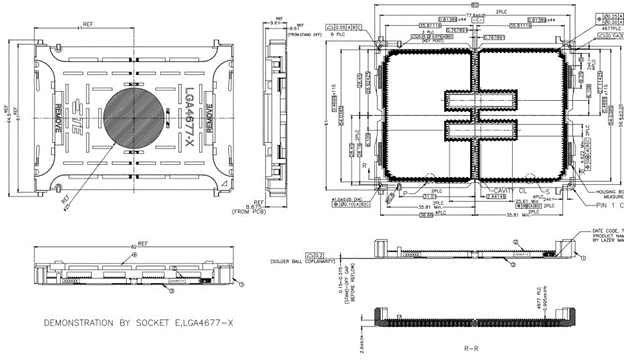
Larger chips are certainly creating interesting design challenges for developers. Here’s an example of the detailed socket LGA 4677 connector:
Typically, a side latch lever holds down the plate and chip, causing the socket contacts to mate simultaneously. This provides an even level of force, which holds the chip pad contacts to the LGA socket connector system.
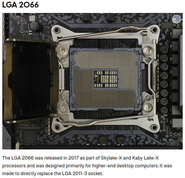
Below is an older LGA 2066 socket connector with a latching frame system:
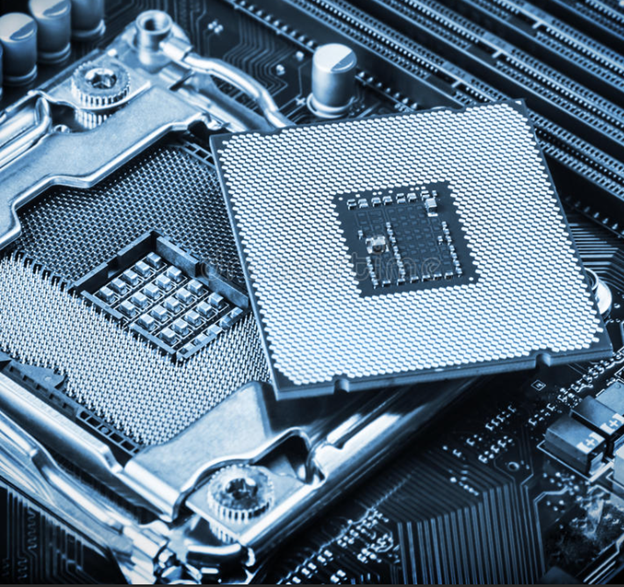
Here’s an Xeon processor chip, with a view from below. The pads have a unique pattern.
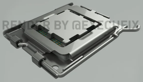
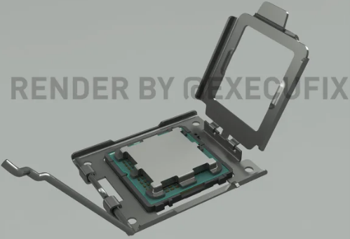
The AMD EPYC Genoa server and AMD Zen 4 “Raphael” CPU’s newest processors will both use the new AM5 LGA socket connector with 1718 contacts.
Check out the LGA socket’s AM5 renderings:
This is the mock-up of the AM5 CPU chip’s bottom side, showcasing the pad array:
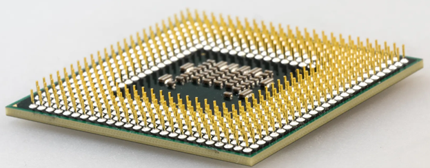
AMD’s server chips previously used LIF PGA socket connectors, such as the AMD AM4 socket connector made by Foxconn below. The side latch lever releases or locks in the internal moving contact structure as a low-insertion force mechanism, which grabs onto the round pins on the base of the PGA chips.
This is the bottom view of an older AMD PGA processor chip, with 1331-pin contacts:
The AMD Zen 4 chip family will likely continue to use the AM5 LGA socket connector rather than the LIF PGA technology sockets that use an LIF lever. Processor chips are more costly today, so it’s ideal to have simple pads on the chips and use bendable copper contacts in the LGA socket connectors.
Additionally, the signaling performance is better with the LGA chip pads and beam tab connectors — at least compared to the process-vulnerable PGA chip round pins and expensive LIF contacts.
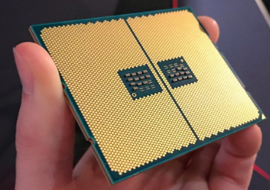
AMD’s Ryzen Threadripper GPU chip uses a new 4094 contact LGA socket connector. It will likely be known as Socket LGA 4094. This GPU chip family also switched from the LIF PGA socket to the new LGA socket with the 4094 flip-chip contact pads.
Here’s an image of its pad array:
And this is the latest generation Socket LGA 4094 connector mounted on a system board:
Market changes
Changes in IO topologies and accelerator interface standards have led to new decisions about which chip socket connectors to use in datacenter applications. This has led to advanced CPUs, DPUs, GPUs, IPUs, and several other new processor device types.
Many IO interfaces like CXL-3, NVLink, and Slingshot now use 8-lane links. Some IO interfaces like PCIe commonly use x16 lane Links and x32-lane port links. This has led to an increase in the LGA socket-pin counts.
Several new datacenter HPC chips now include a collection of compute chip tiles and multiple IO interfaces, which are incorporated into one substrate module. Some of these chips are LGA sockets; others are edge-connector modules.
Given the various IO interfaces, shrinking link reaches, and increasing speed rates, the market could use new solutions.
TE’s ChipConnect assemblies are one solution that offers LGA-3647 socket connectors with internal twin-axial cable-to-faceplate internal IO receptacle connectors, like the QSFP.
This is a newer application family that seems to offer market growth potential, but forecasting is held tight.
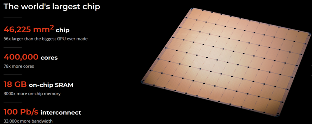
Wafer Scale Engine or WSE chips are many times larger than the current high-circuit count CPUs, GPUs, and IPU chips (which mostly use LGA socket connectors). Most of the system connectivity is done within the chip’s silicon layers. Only some of the IO lines are brought to the two sides, which include 10-edge connectors.
This is Cerebras’s extremely large chip, currently the world’s largest, according to the company:
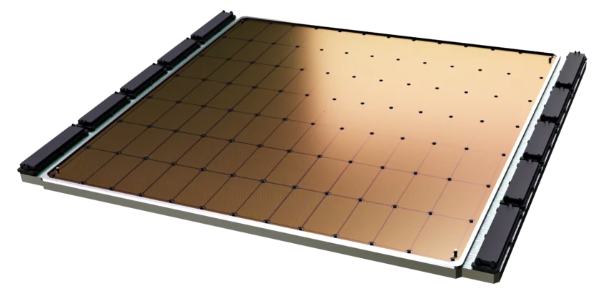
Connecting this large chip to the rest of the system is a challenging design process. A matching cold plate supports the wafer chip’s assembly as shown below. Ten black IO edge connectors are also used on each side of the assembly. This device is packaged as a removable module. Click here to learn more.
Accelerator IO high pin-count chips (and others) are increasingly mounted on a special module substrate. This module assembly is typically plugged into a high-speed edge connector rated for 112G PAM4 performance. There has been a proliferation of different custom and standard edge connectors, pin counts, contact pitches, and form factors supporting such solutions.
Several global and Tier 1 developers have initiated a new OCP Accelerator Module standard and specification. The high pin-count processor chips might be mounted differently to this module board, but many Accelerator products will use the new OCP standard connector and specification.
But could newer CPU products also use this open-module technology? That would require the support of even more pins per connector.
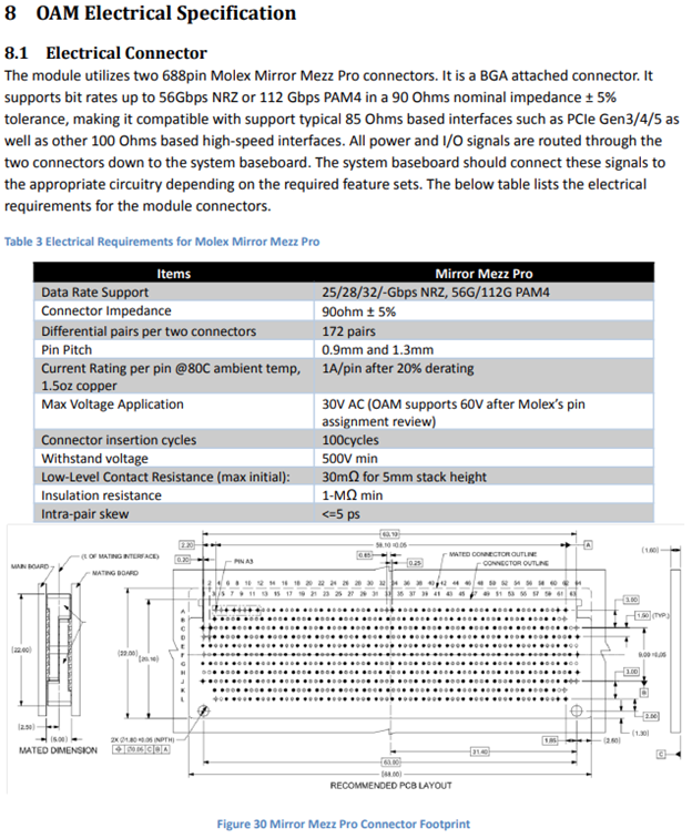
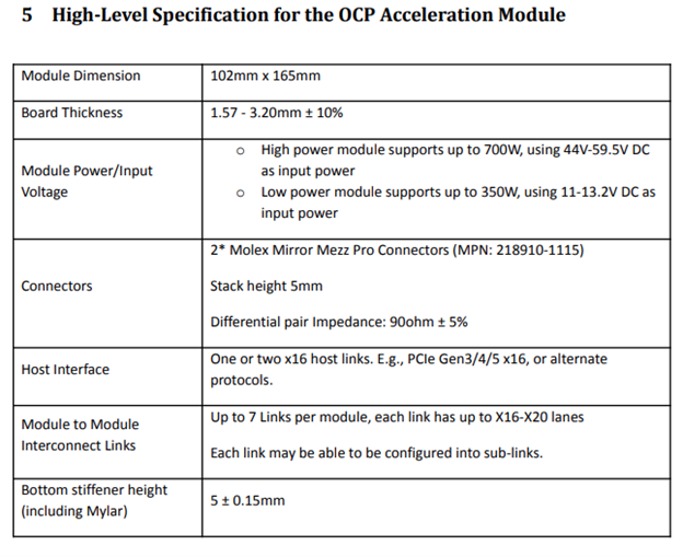
The OCP Accelerator Module, QAM, supports high-speed 1 or 2 x16 links, 1-7 x16 links, as well as other high-speed links. Each connector provides 172 differential pairs of 90 Ohm performance using two mated mezzanine connectors. This equates to 344 pairs.
The new specification calls for using two Molex Mirror Mezz connectors. This was selected and implemented by the OCP committee. The specification adoption rate is growing for many end-users market segments. There are also several new private module applications.
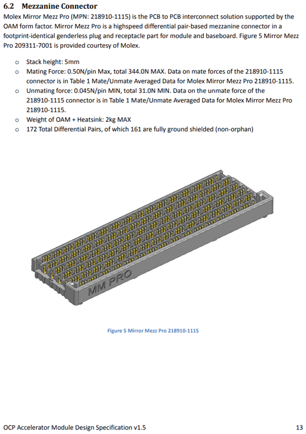
OCP OAM Mezzanine connector
Here’s a look at the Molex Mirror Mezz Pro, 5mm stacking height connector, with key specification information:
Technical challenges
The pad-on-beam contact engagement has been historically reliable, but each new generation requires more contacts, running at different impedances and with other thermal requirements.
Currently, the LGA connectors use up to 4677 pins, increasing the total ganged device insertion force. The normal force of the bendable beam contact must be designed so that it mates well in terms of wipe distance, overall coplanarity, and SI symmetry with each pad contact of the OAM or other CPU module.
Aside from thousands of tiny contacts, the typical LGA socket connector uses levers, back plates, bolster plates, clips, carriers, and cover components that support product performance and lifecycle testing.
Questions
Will the HPC DC market move to use new high-performance connector and cabling solutions or continue to use commodity server socket connectors, internal cables, and external cable interconnect?
What will the next generation of LGA socket connectors look like for Intel’s Granite Falls 3nm CPU processor chip, expected to hit the market in 2024?
Will liquid cooling and socketing of future processor chips be more integrated?
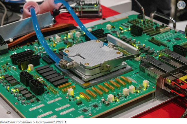
We still have many questions. For now, here’s the new high-speed Ethernet switch chip. It’s being liquid cooled with a top-mounted system:
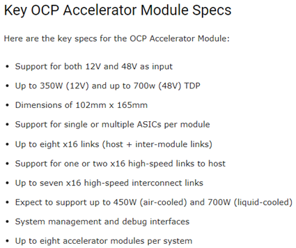
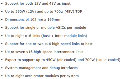
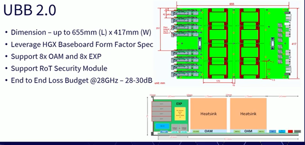
Below are some spec highlights affecting the OCP QAM mezzanine connectors and the OCP UBB main assembly:









Leave a Reply
You must be logged in to post a comment.